Matsuoka Lab. New Industry Creation Hatchery Center Takashi Matsuoka Emeritus Professor of Tohoku University
Overview of Research on Distributed Feedback Laser Diode in the wavelength of 1.55 μm
Study of distributed feedback semiconductor lasers in the long wavelength region
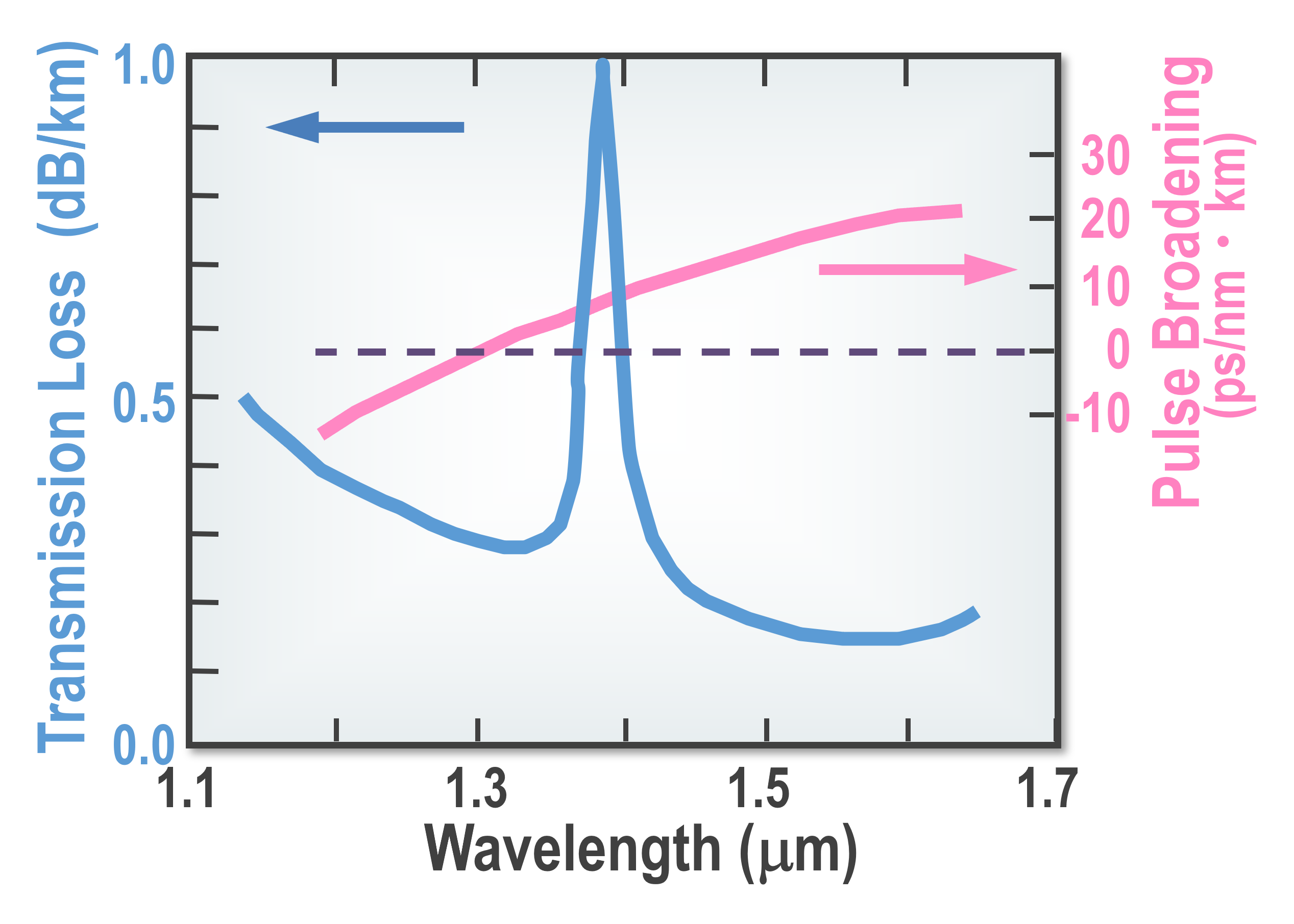
Fig. 1 Transmission loss of optical fiber and wavelength dispersion of optical pulse broadening
H. Kawaguchi et al., Electron. Lett., 15 (1979) 669.
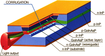
Fig. 2 Structure of DFB Laser Diode
Conventionally, Fabry-Perot (FP) lasers, which shows multi-longitudinal mode oscillations, have been used as light sources for optical communications systems. For including light with different wavelength in a pulse signal, the pulse width is broadened during transmission due to the wavelength dispersion of the propagation. In the system of the pulse interval shortened or the transmission with long haul, the successive pulses become overlapped during the transmission. This phenomenon limits the high bit-rate and long-haul transmission.
Instead of this FP laser, the distributed feedback laser as one showing single-longitudinal- mode oscillation was studied. This laser has corrugation with the period of 240 nm as an optical filter under the emitting layer.
A DFB laser was studied by using GaAs and related materials in 1970s. It could not be used because of its short device lifetime. Its characteristics were not sufficiently analyzed. In these situation, both techniques of the epitaxial growth and the fabrication process were established. In 1981 the first continuous-wave (CW) oscillation at room temperature was successively realized.
T. Matsuoka, H. Nagai, Y. Itaya, Y. Noguchi, Y. Suzuki and T. Ikegami, Electron. Lett.,18, .27 (1982).
Development of DFB LDs
Before Matsuoka's work
GaAs
1971
Principle confirmation of Distributed Bragg Reflector (DBR) laser by Kogelnik et al. (AT&T Bell Labs)
1972
Theory of DFB laser by Kogelnik et al. (AT&T Bell Labs)
1973
Couple mode theory Yariv (Caltech)
1974
Research on the theory of the effect in the corrugation phase at the end facet by W. Streifer (Xerox)
1975
Room-temperature CW oscillation of GaAs/GaAIAs DFB laser diode by M. Nakamura et al.(Hitachi, Caltech)
InP
1980
Pulsed Operation of lnGaAsP/lnP DFB laser diode by 0. Mikami (NTT)
Matsuoka's works
1981
First CW operation at room temp.
1983
Development of etchant suitable for nm-order microfabrication
Suppression of thermal deformation of corrugation during epitaxial growth
1984
Experimental confirmation on effect of corrugation phase at the facet and proposal of LD structure for SLM oscillation
1985
Prediction of temperature range in SLM oscillation
Design of LD structure for high-efficiency, low threshold current and high yield in fabrication yield
1986
Light output power of 45 mW under CW operation at room temp.
Later, the device characteristics were precisely analyzed. Based on these analyses, the structure with high yield of SLM oscillation was designed. This DFB LDs were supplied to the researchers in the field of the optical communications systems, and as a result DFB LDs were useful for the optical communications systems since 1982. From 1983 to 1985, the fabrication technique of DFB LDs was transferred to a few deice makers.
Presently, DFB LDs have been widely used as light sources for high-bit-rate and long-haul optical communications systems in Japan, Europe, and USA. In Japan, ese system, the system over ten thousands km has been constructed. Its bit-rate is 100Gb/s per wavelength. Based on the characteristic of SLM oscillation, the concept of the wavelength division multiplexing (WDM) system has been created, and the 100-wavelength multiplexed system has been realized. Its bit rate reaches to 10Tb/s per fiber. This value corresponds to 1.56 G lines of conventional phones. It is not too much to say that DFB LDs have supported the advanced information society.
ECOC prize as the best paper award of European Conference on Optical Communications (ECOC), which was one of three biggest conferences on communications systems, was awarded in 1984.
Fig. 3 Optical fiber submarine cable through North Pole
IEEE Spectrum, Jan. 15, pp. 11-13 (2015).
The research issues studied are concretely shown below.
Table 1. Key technologies for fabricating DFB LD
Technique
Issue
Technology before my work
Fabrication of Corrugation
Design and Construction of Dual-Beam Interferometer Pattern width: 0.12 µm
Minimum pattern width: 2 μm
Photolithography photoresist thickness 30 nm
Minimum photoresist thickness: 0.5 μm
Etchant for lnP: Development of stable etchant without generation of bubbles
Hydrochloric acid: Unstable with generating bubbles
Epitaxial Growth
Cleaning of Corrugation Surface
Liquid Phase Epitaxy(LPE)
Keeping Corrugation Shape during Epitaxial Growth
No experience
Device Design
Design of Corrugation Shape
Couple-mode theory
Probability of Single-Longitudinal-Mode Oscillation
No discussion
Starting the research on October, 1980
Development of exposure system consisted of two-beam interferometer system
Fig. 4 Principle of exposure system consisted of two-beam interferometer systemFig. 5 Externally sailed equipment of exposure system consisted of two-beam interferometer system
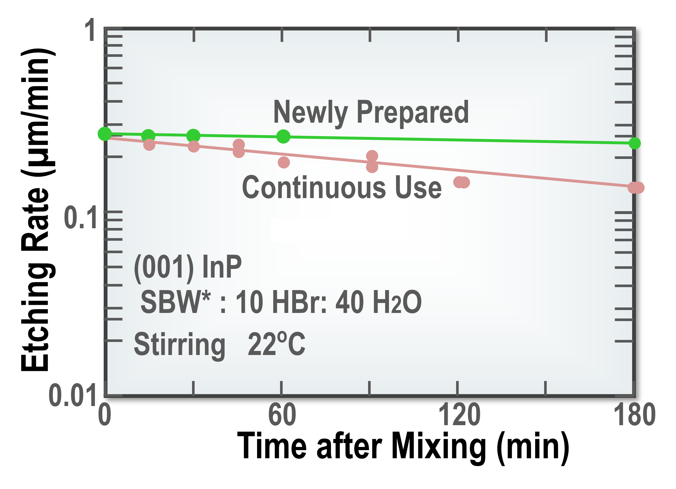
Development of etchant with high controllability and reproducibility for processing InP
Fig. 6 Stability of Developed etchant for (001) InP substrate SBW*:10HBr:40H2O
*SBW: Saturated Bromine Water
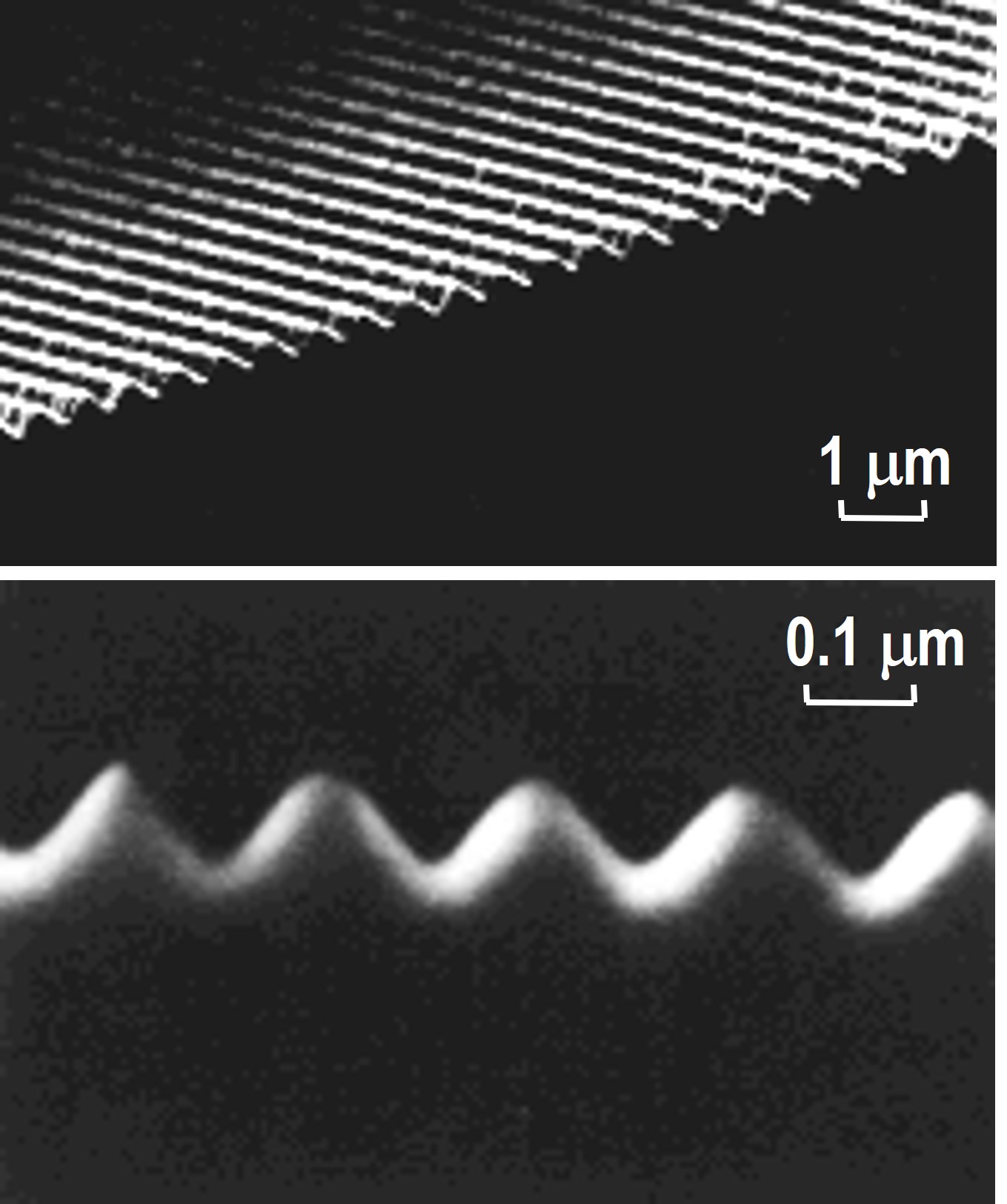
Fig. 7 SEM Photographs of corrugation with period of 197 nm formed on (001) InP substrate
Ref. T. Matsuoka and H. Nagai, J. Electrochem. Soc. 133, 2485 (1986).
Development of the technique suppressing the thermal deformation of InP corrugation
When the device structure is grown pn the InP corrugation, the corrugation was thermally deformed in the reactor of a liquid phase epitaxy (LPE) system during the soaking duration in the reactor. This phenomenon was analyzed based on the thermal dynamics. Finally, to introduce a phosphine gas into the growth ambient, the device structure as successively grown without deformation.
Fig. 8 Principle of mass transportFig. 9 Effect of introducing PH3 into LPE reactor
Fig. 10 Cross-sectional view of DFB-LD structure grown on corrugation
ref. H. Nagai, Y. Noguchi, and T. Matsuoka, J. Crystal Growth 71, 225 (1985).
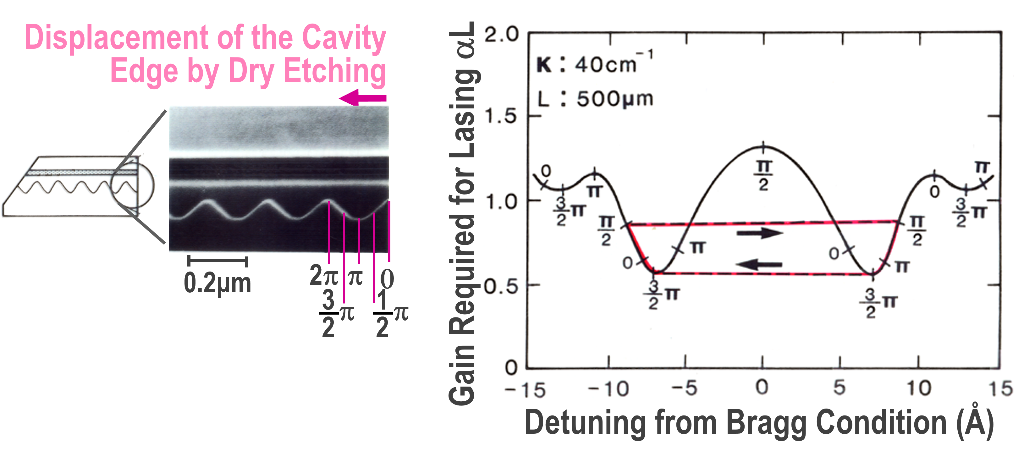
Effect of corrugation phase at the cavity facets
While changing the corrugation phase at the cavity facet by directly etching the cavity facet was changed, the device characteristics were measured. The characteristic of SLM oscillation was pointed out to depend on the corrugation phase at the facet.
Fig. 11 Effect of corrugation phase at the cavity facet
Ref. T. Matsuoka, H. Nagai, and Y. Yoshikuni, IEEE J. Quantum Electron., QE-21, 1880 (1985)
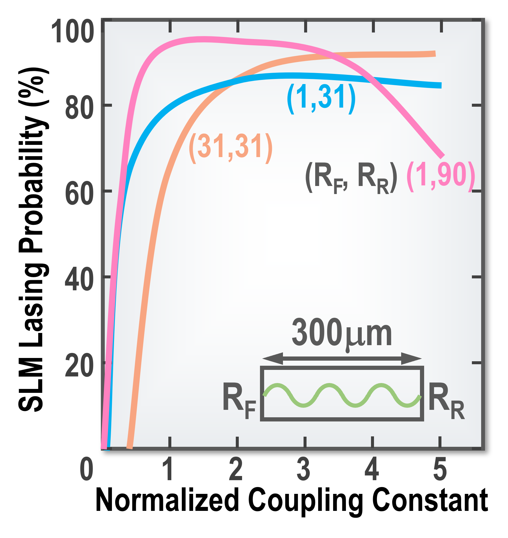
Device design
Fig. 12 Device structure of DFB LD and probability of SLM oscillation
The device structure of DFB LDs with high yield fabrication, high output power, and stable operation was designed through the analysis based on the couple mode theory considering the corrugation phase at the cavity facet.