
Beginning
I noticed that GaN had the crystallographic polarity when I epitaxially grew GaN on SiC substrates with hexagonal structure as shown in Fig. 1 (T. Sasaki and T. Matsuoka, "Substrate-Polarity Dependence of Metal-Organic Vapor-Phase Epitaxy-Grown GaN on SiC", J. Appl. Phys., 64, 4531 (1988)).
T. Sasaki and T. Matsuoka, "Substrate-Polarity Dependence of Metal-Organic Vapor-Phase Epitaxy-Grown GaN on SiC", J. Appl. Phys., 64, 4531 (1988).
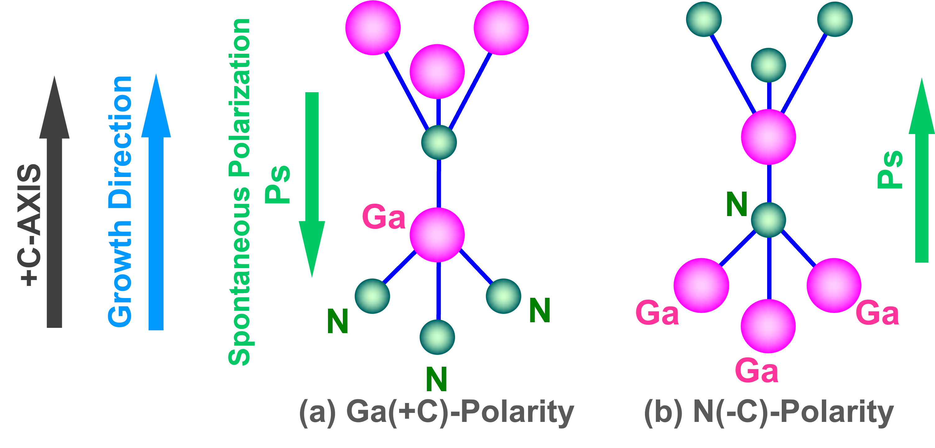
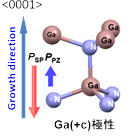
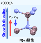
In usual epitaxial growth of GaN on any substrates, Ga-polar growth has been used. In this polarity, one nitrogen atom is captured with only one Ga atom on the top surface of the growth. On the other hand, for the nitrogen-polar growth, one nitrogen atom is captured with three Ga atoms. Form this difference, a nitrogen atom can be easily captured in nitrogen-polar growth. Among three termination materials constructing InGaAlN, i.e., AlN, GaN, and InN, InN has extremely higher equilibrium vapor pressure of nitrogen in comparison with other GaN and AlN. This leads to make InN difficult to be included into InGaAlN. My lab. succeeded in the first epitaxial growth of N-polar GaN (T. Matsuoka, T. Mitate, H. Takahata, S. Mizuno, Y. Uchiyama, A. Sasaki, M. Yoshimoto, T. Ohnishi, and M. Sumiya, "N-Polarity GaN on Sapphire Substrate Grown by MOVPE", Phys. Stat. Sol. (b), 243, 1446 (2006).
. In this figure, the spontaneous polarization is also pointed out. Its direction is inverted dependently on the polarity. This physics can be effectively used in the device design as mentioned in the above paper. I have planned our future research based on this technique.
We corrected the band-gap energy of InN by the first success of single crystalline InN epitaxial growth (T. Matsuoka, H. Okamoto, M. Nakao, H. Harima, and E. Kurimoto, "Optical Band-Gap Energy of Wurtzite InN", Appl. Phys. Lett., 81, 1246 (2002).). Still now, the characteristics of In-rich contained material have been unknown. The investigation of their characteristics is very meaningful from the view point of device applications. We corrected the band-gap energy of InN by the first success of single crystalline InN epitaxial growth (T. Matsuoka, H. Okamoto, M. Nakao, H. Harima, and E. Kurimoto, "Optical Band-Gap Energy of Wurtzite InN", Appl. Phys. Lett., 81, 1246 (2002).). Still now, the characteristics of In-rich contained material have been unknown. The investigation of their characteristics is very meaningful from the view point of device applications. The direction of polarization is inverted between Ga-polarity and N-polarity as shown in Fig. 1. We’d like to apply this concept to devices. For an example, an N-polar grown solar cell has much higher characteristics than Ga-polar one as shown in Table. 1 (T. Tanikawa, J. H. Choi, K. Shojiki, R. Katayama, and T. Matsuoka, "Demonstration of N-Polar InGaN/GaN MQW Solar Cells", 6th World Conference on Photovoltaic Energy Conversion (WCPEC-6), 1TuPo.2.16 (Kyoto, Japan, Nov.24-27, 2014).). Nitride semiconductors is expected to be applied to high-power and high-voltage devices, in particular, longitudinal type transistors. For realizing these applications, GaN wafers with low density of dislocations are indispensable. Ammonothermal method for bulk growth of GaN with high quality has been studied for a long time. However, for mass-production, this method has not been successful yet because the growth rate is too small. As a method with high growth rate, halide vapor phase epitaxy (HVPE) is expected. When a thick GaN is epitaxially grown on a Ga-polar GaN base-wafer, its shape becomes taper. This means that we cannot obtain large-diameter-GaN wafers. For N-polar growth, the diameter is extended during growth. Therefore N-polar HVPE can be hopeful for mass-production. Growth of In-rich InGaN and its characterization
Device applications of polarization inversion
Orientation
Band Diagram of Solar Cell Structure
Extraction Efficiency
Ga-polar (Ga face)
.png)
Poor
Polarization Electrical Field prevents the Extraction of photo-generated carrier.
N-polar (N face)
.png)
Good
Polarization Electrical Field enhances the Extraction of photo-generated carrier.Challenge to Bulk GaN Fabrication