Introduction of the outline of the research carried out throughout the days of NTT Laboratories and Institute for Materials Research, Tohoku University.
Room Temperature CW Operation of InGaAsP/InP DFB Lasers
As a light source for high bit-rate and long haul optical communications systems, a distributed feedback (DFB) laser with an InGaAsP/InP double heterostructure was studied for fabricating a semiconductor laser operated with single-longitudinal-mode (SLM) oscillation. This DFB laser had a corrugation with pitch of 200 - 240 nm as an optical filter under the emitting layer.
A DFB laser was researched to be fabricated with GaAs material system in 1970s, unfortunately, its device lifetime was too short to be used for communications systems. Its characteristics were not analyzed, neither. T. Matsuoka established the crystal growth and the device fabrication process, analyzed the device characteristics, and proposed the device structure with high probability of SLM oscillation. In 1981, he succeeded in the first continuous wave (CW) oscillation of DFB laser in the wavelength region of 1.5 µm.
Pressurized MOVPE Growth of InN and Optical Devices Applications
Indium containing InGaN alloy is a well-known and promising material for high-brightness blue, green and white light emitting diodes (LEDs) as well as for blue-violet laser diodes (LDs). Currently the InGaN LEDs are widely used as the traffic signs and white back lights of the liquid crystal display in the smart phones. However, the physical properties of the terminal alloy, InN, are still unknown, since it is difficult to grow high-quality InN films which are durable for the characterizations, due to the extremely-high equilibrium vapor pressure of nitrogen from InN at the standard growth temperature. In our laboratories, the specially-designed pressurized MOVPE reactor, which can be operated up to 4 atm, had been introduced to clear up the problems and successfully realized the epitaxial growth on InN films*1. We found the interesting properties such as the bandgap energy located at the NIR regime and its low sensitivity to the temperature*2 *3, which are suitable for the optical fiber communications system superior to the widely-used LDs based on InGaAsP/InP. We are continuing to develop the novel LDs made of InN and related nitride semiconductors.
Development of N-polar InGaN Devices
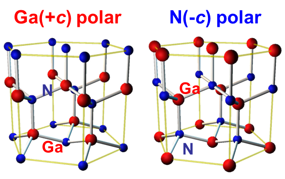
Our group succeeded in the growth of high-quality N-polar nitride films with opposite crystallographic orientation against widely-used Ga-polar counterparts. If you flip the crystallographic orientation, it is expected that the growth habits and the potential device structures should be completely modified, since the physical properties and the chemical stability of two opposite faces differ significantly with each other. In this work, the effects of the polarity on the growth evolution and device performance as well are clarified carefully, in order to realize much higher efficiency InGaN-based devices never achieved by commonly-used Ga-polar orientations.

Exploration of Exotic Substrate and Processes
In usual case of nitride LEDs, c-plane sapphire (Al2O3) is used as the substrate due to the commercial availability, while the crystal quality of the nitride films on the sapphire substrate is not enough since its in-plane lattice constant differs from that of nitride crystals significantly. As for the cleavage habit, easy-cleavage planes for nitrides and sapphire are different with each other, and the fabrication of cleaved-facet cavity mirror for LDs is impossible. Considering the above two issue, currently available blue-violet LDs are grown on the lattice-matched bulk GaN substrates. However the GaN substrates, whose growth process is still under the development, are very expensive and hard to process. So we are now trying to replace with other exotic materials and processes.
Physics of Widegap Semiconductor Photonic Nanostructure
Previous research on nitride semiconductors mainly focused on the development of the high-efficiency light-emitting devices based on the direct inter-band emission. However, these widegap materials have a number of interesting physical properties such as strong optical nonlinearity and extremely stable exciton, most of them were still untouched by the device developers. So in this work we are trying to propose novel optical devices and systems by squeezing out the above promising and hidden physical properties.
