T. Matsuoka, H. Tanaka, T. Sasaki, and A. Katsui, International Symposium on GaAs and Related Compounds (Karuizawa, Japan, Sept. 25-29, 1989); in Inst. Phys. Conf. Ser., 106, pp. 141-146 (1990).
T. Matsuoka, MRS Internet J. Nitride Semicond. Res. 3, 54 (1998).
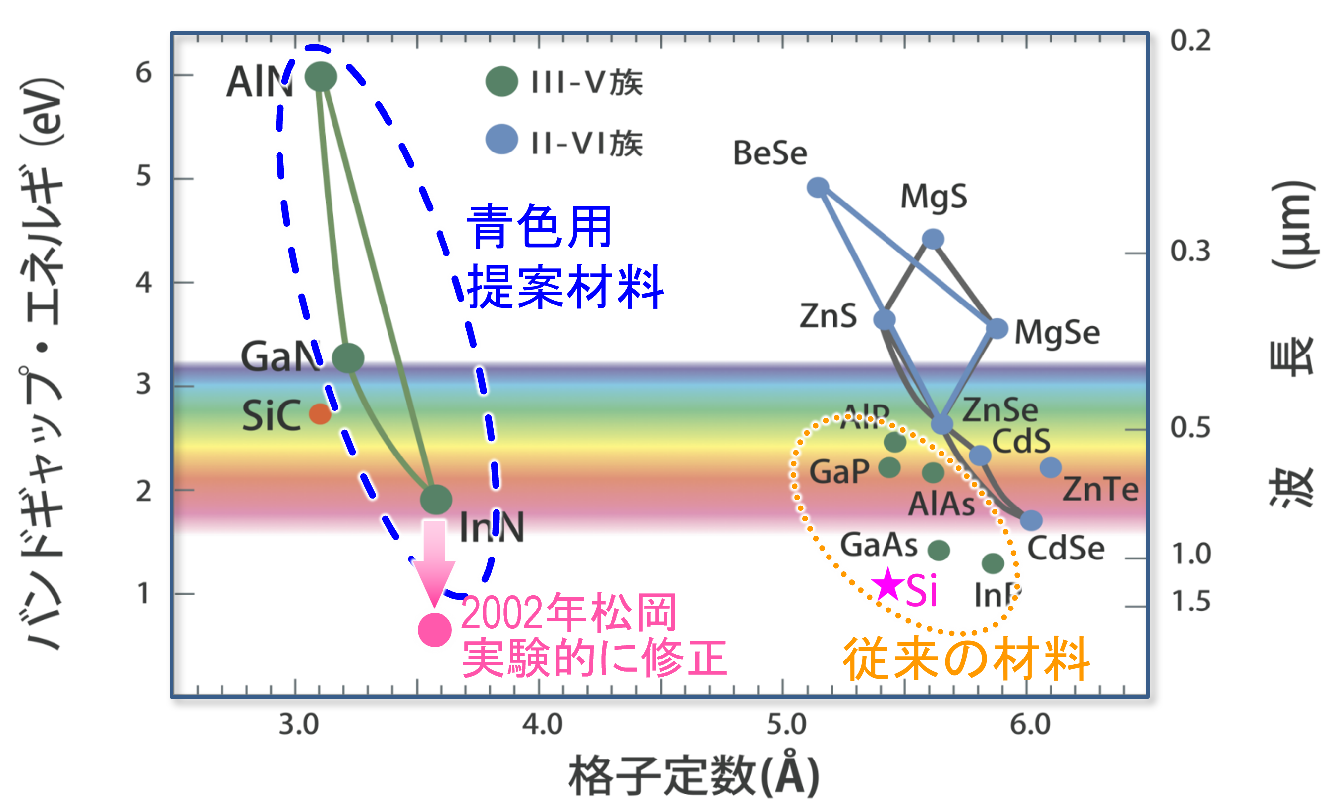
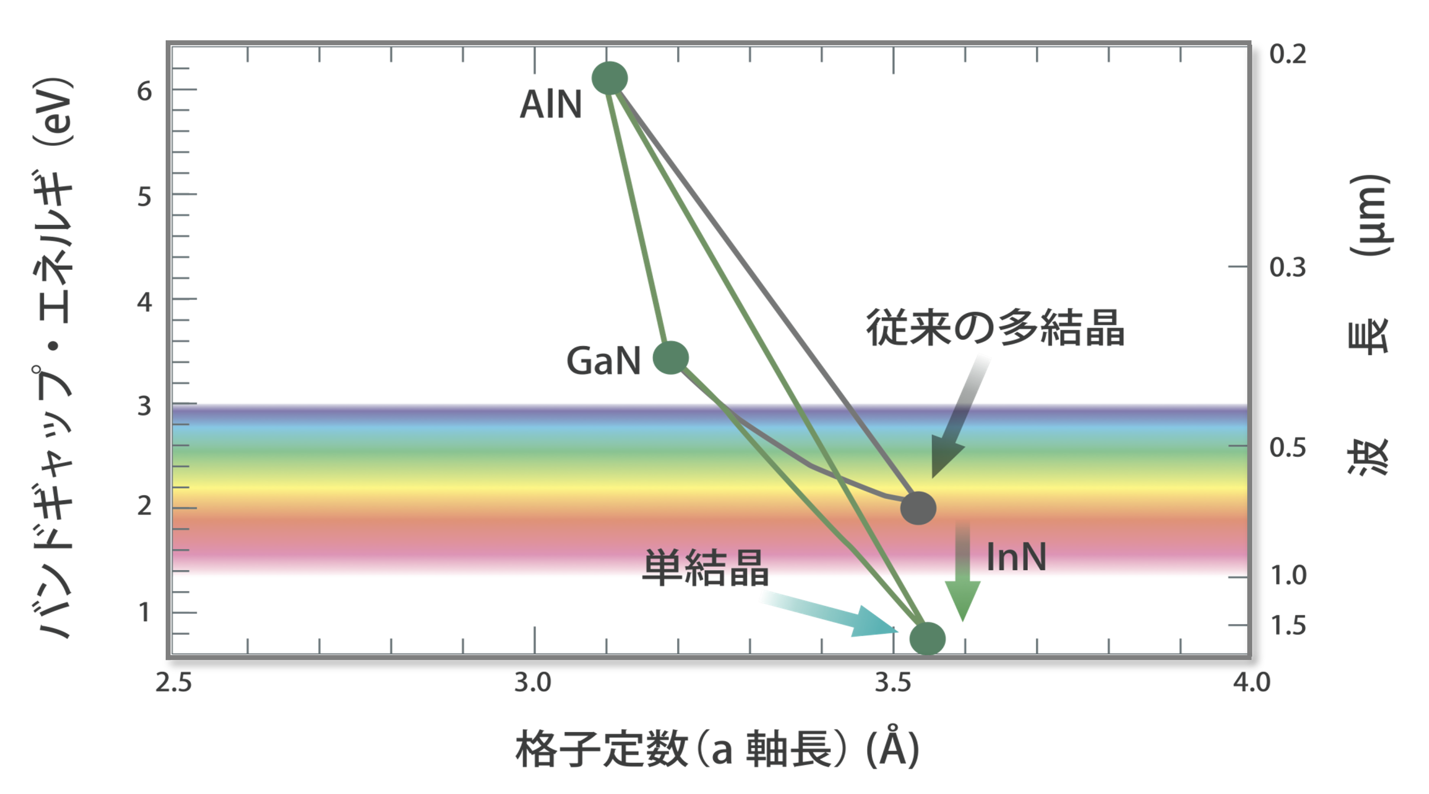
InNのバンドギャップ・エネルギーの予測
四元混晶InGaAlNの提案の際に下記の記述をしています。
International Symposium on GaAs and Related Compounds (Karuizawa, Japan, Sept. 25-29, 1989); in Inst. Phys. Conf. Ser., 106: Chaptor 3, pp. 141-146 (1990).
Wide-gap semiconductor (In,Ga)N
T. MATSUOKA, *H. TANAKA, T. SASAKI and A. KATSUI
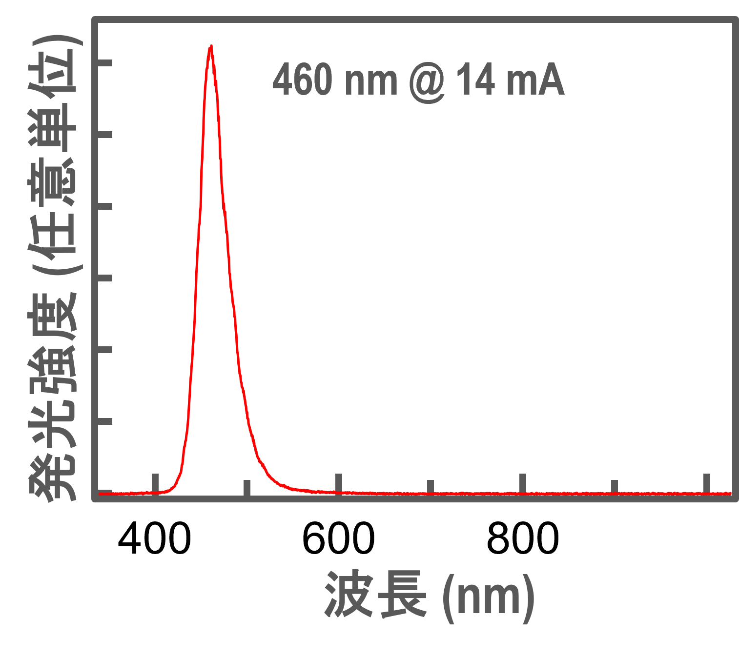
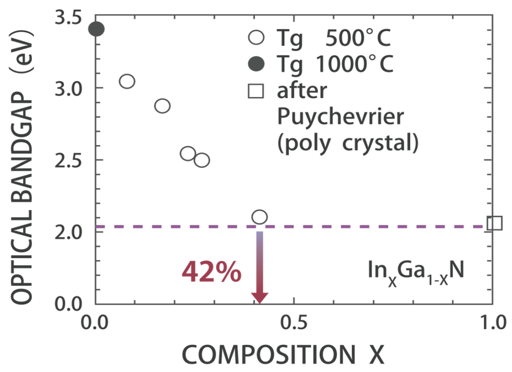
Fig. 9 Relationship between InN mole fraction x and optical bandgap.
Only (In,Ga)N layers with unambiguously determined optical bandgap are shown in this figure. Only GaN was grouwn at 1000°C. The measured optical bandgap of GaN almost coincides with the reported value (Monemar 1974). In this figure, the optical bandgap of poly-crystal InN from the literature (Puychevrier 1976) is also shown.This value is almost same as taht of (In,Ga)N with 0.42 of InN mole fraction.
Q. Guo et al., Jpn. J. Appl. Phys., 33, 2453 (1994).
InNの光通信応用
高密度多重化のメリット
短距離
基幹系
次世代
光源材料
InGaAsP/InP
InN/InGaAlN
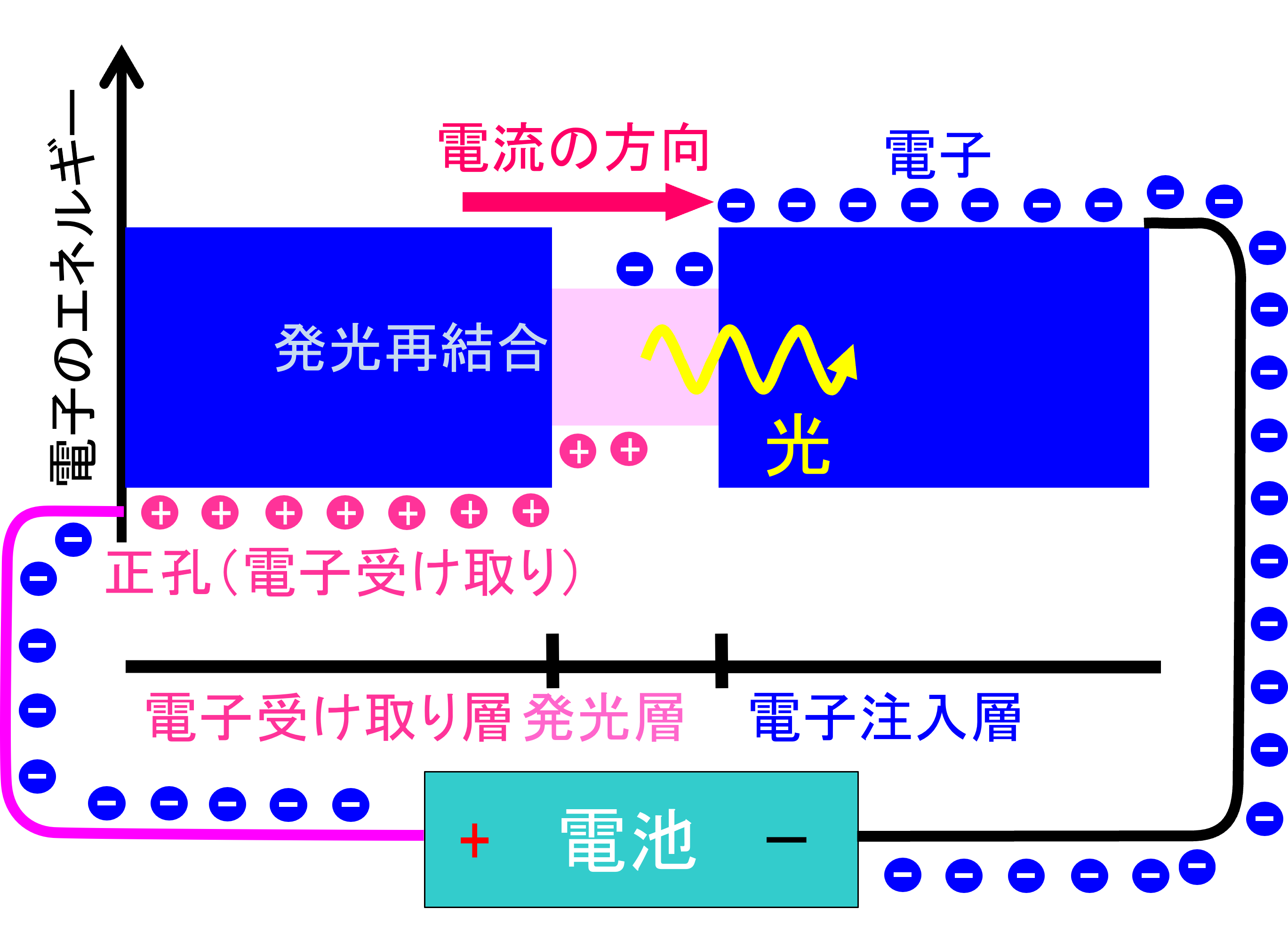
素子構造
(FP) LD
DFB LD
DFB-LD
伝送容量/1波
400 Mbps
100 Gbps
100 Gbps
多重化システム
なし
C-WDM
D-WDM
多重度 (WDM)
1
100
1000
波長間隔
—
4- 8 nm
0.4 - 0.8 nm
伝送容量/1芯
400 Mbps
10 Tbps
100 Tbps
白色LED
白色光源の効率
疑似白色光源を含めた、各種白色光源の発光効率を比較を図xxyに示す。
各種白色光源の効率
LEDの省エネ効果
照明で消費する電力は総発電量の 25 - 40 %
世界におけるLEDの節電効果
西暦
2005
2010
2015
2020
2025
照明のLED率 (%)
2005
2010
2015
2020
2025
削減電力量 (× 1012 Wh/年)
2
67
330
720
1,100*
コスト (× 億円/年)
224
7,504
36,960
80,640
123,200
* 日本国内の年間総発電量に相当
R. Haitz, F. Kish, J. Tsao, and J. Nelson, SANDIA REPORT, SAND2000-1612 (2000).
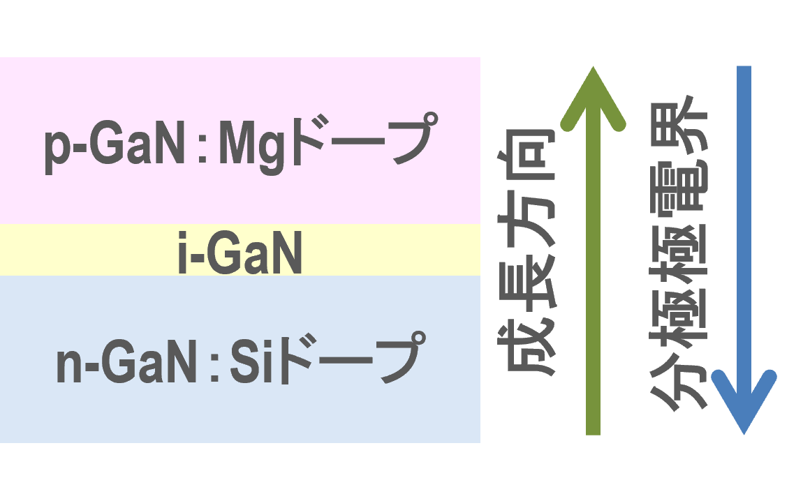
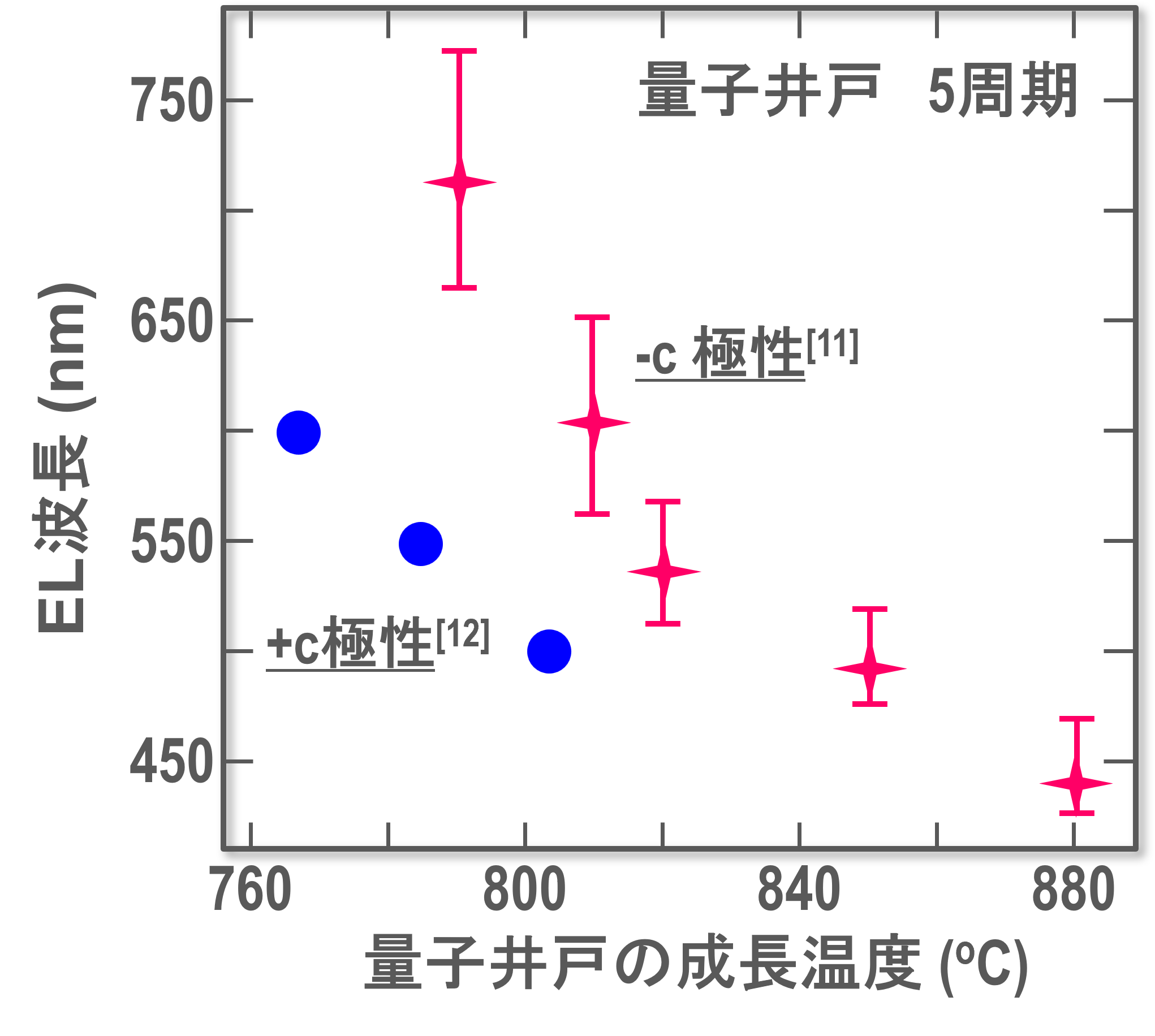
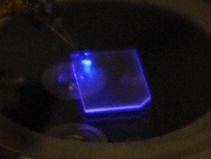
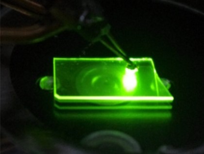
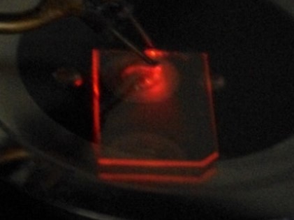
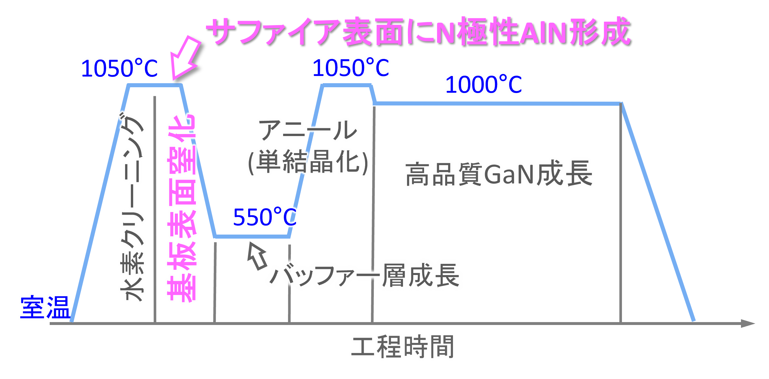
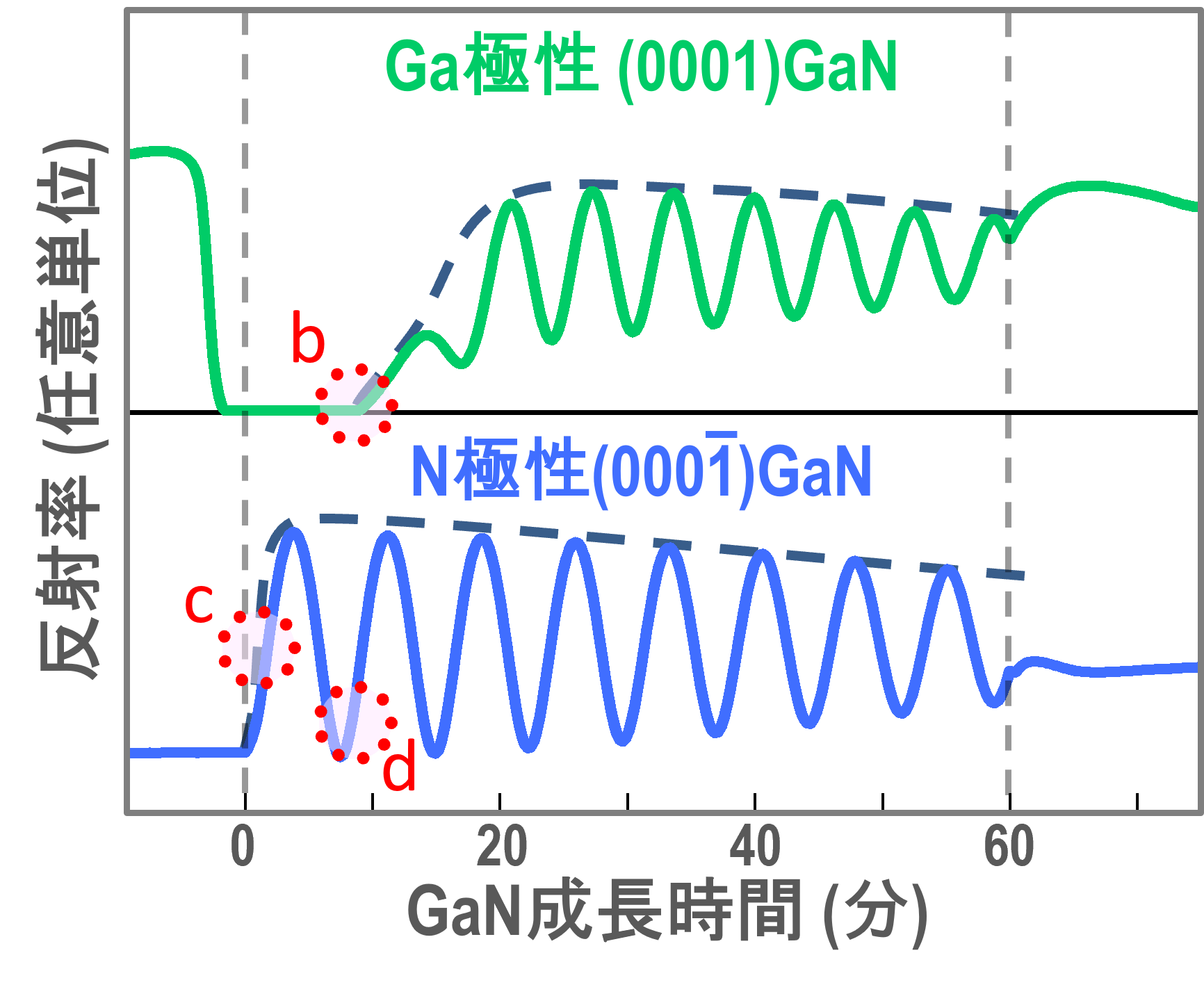
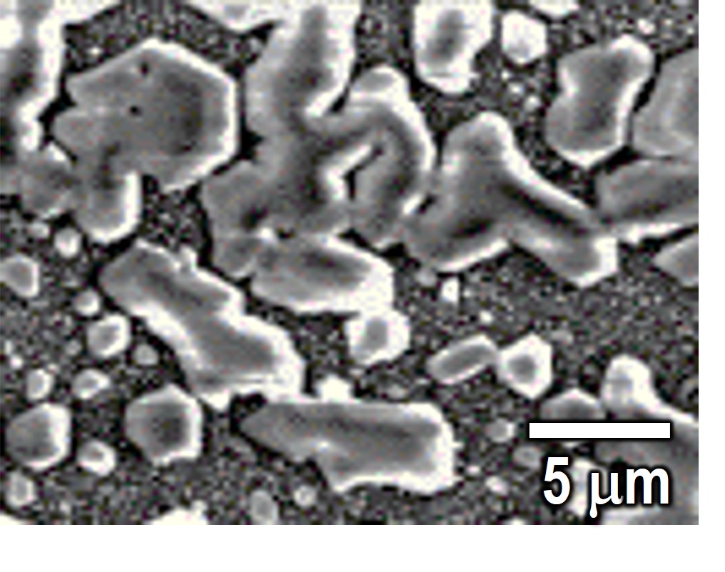
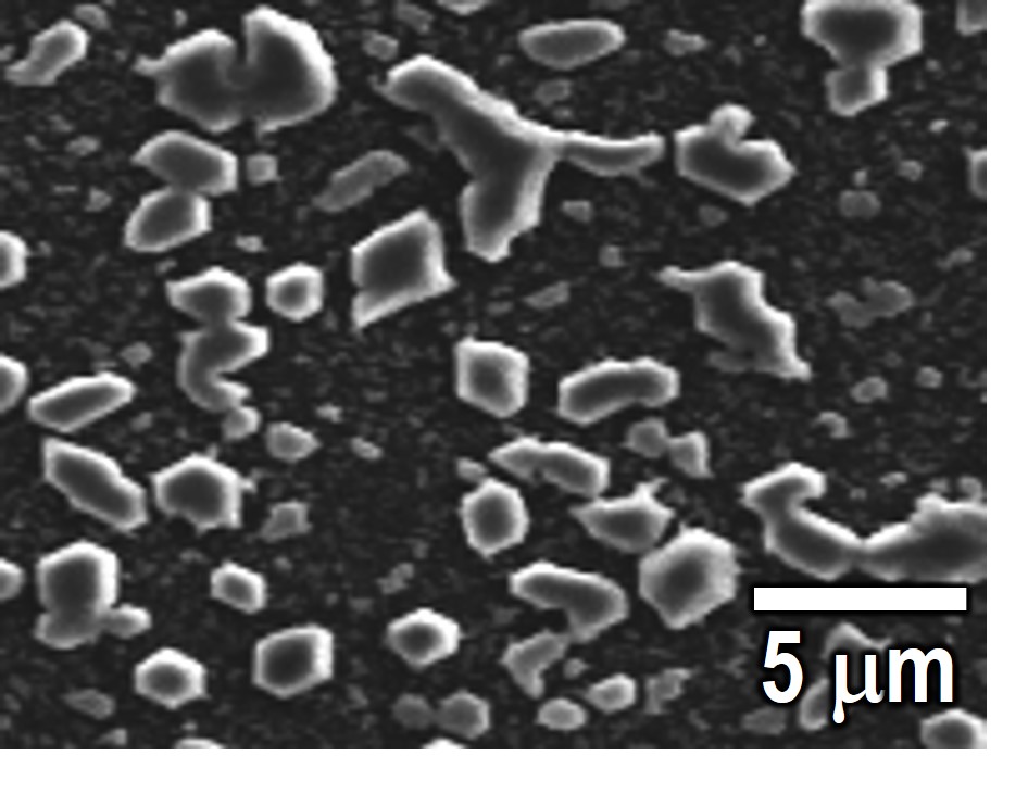
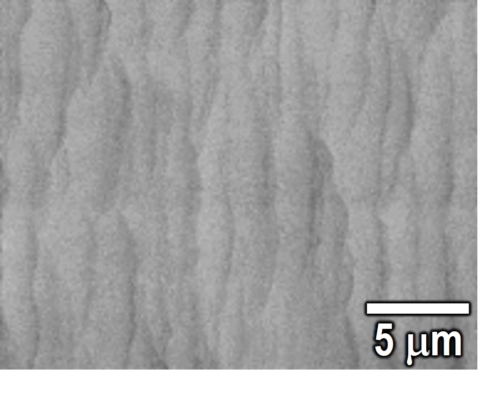
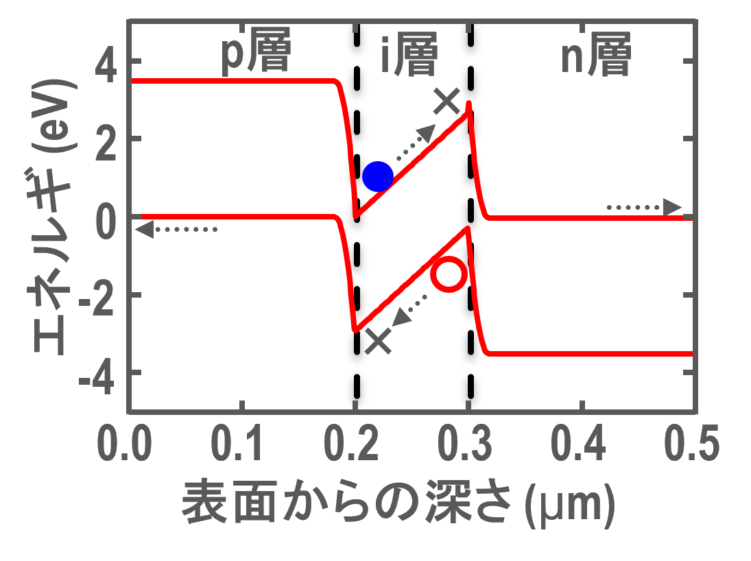
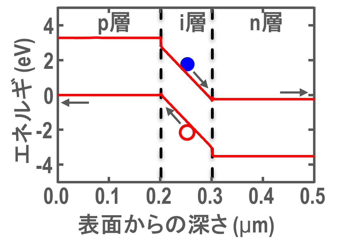
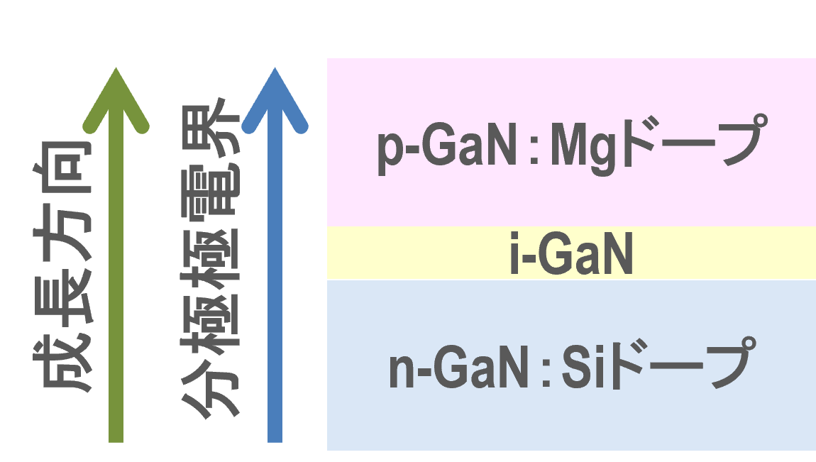
窒素極性成長
きっかけ
Ga (+C) 極性N (-C) 極性
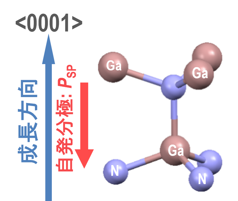
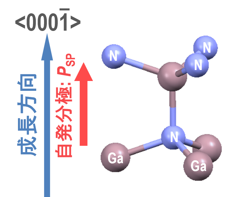
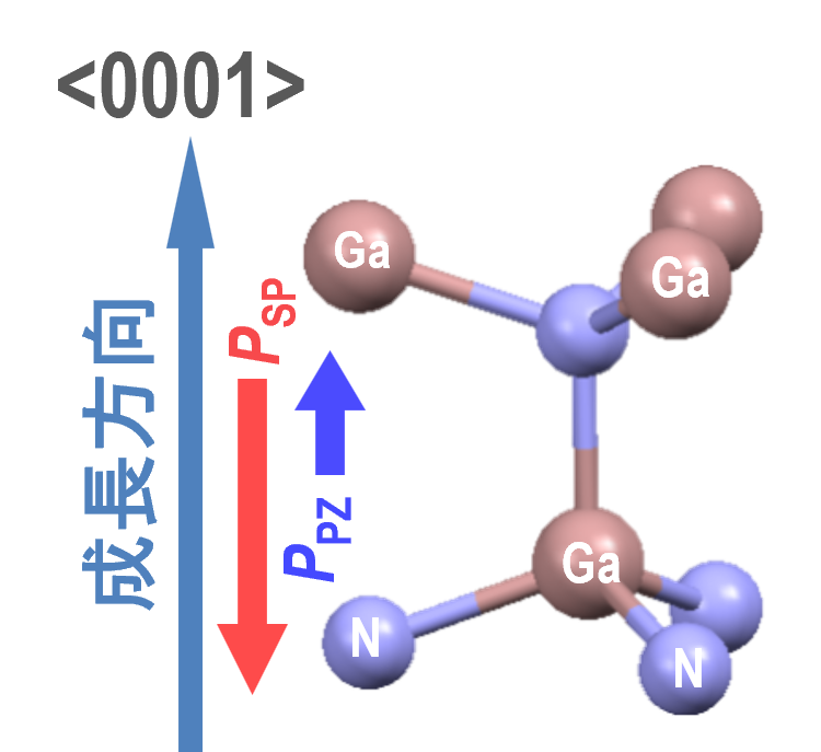
ウルツ鉱型GaNにおける結晶の極性と分極
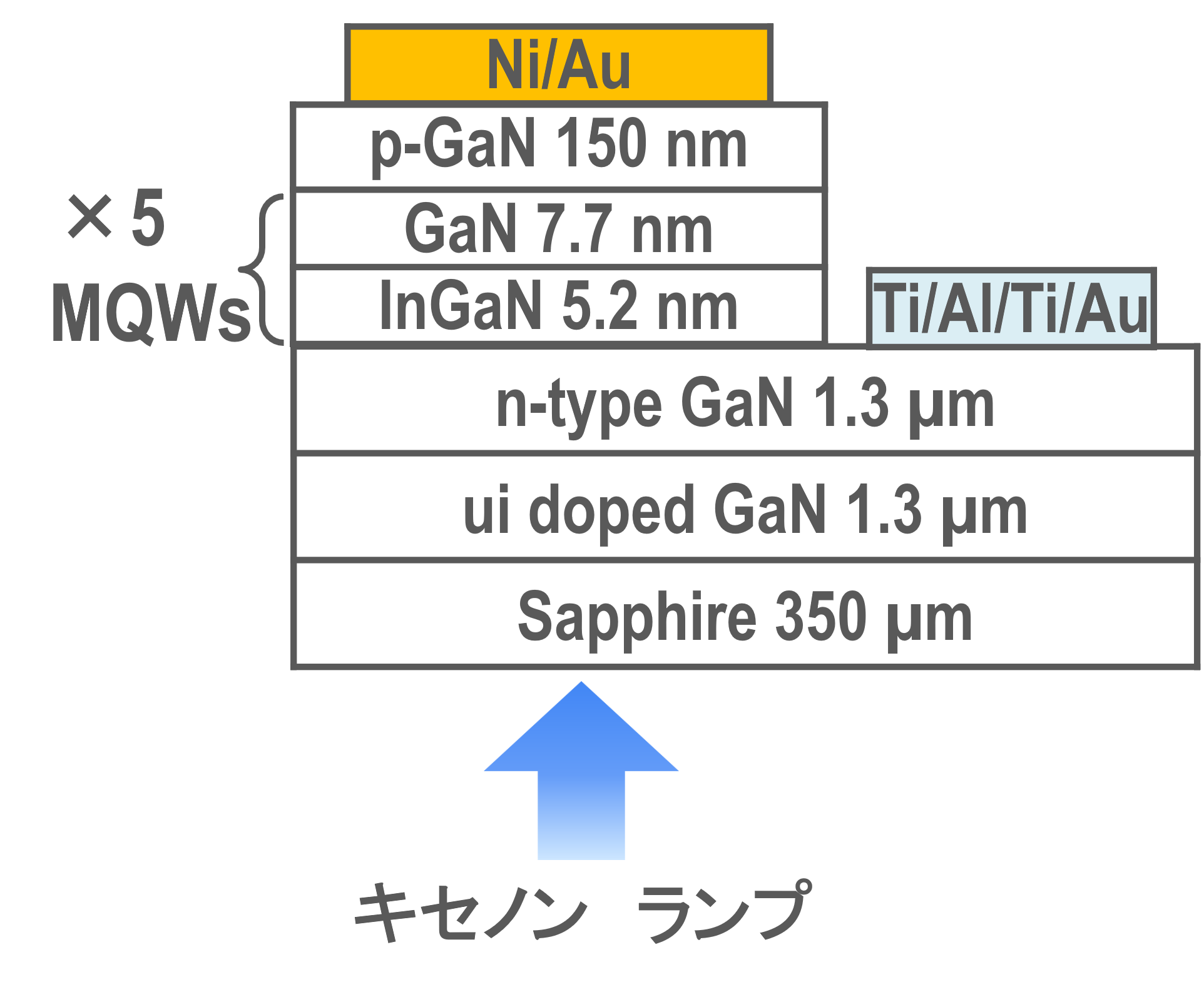
六方晶系のSiC基板上にGaNを成長したときに、図 9.に示す極性に気づいていました。
GaN was grown on the basal planes of SiC by MOVPE. The surface morphology and luminescence property are strongly dependent on the substrate polarity. Differences in the binding-energy shifts of the Ga photoelectron spectra lead to the conclusion that GaN epitaxial layers on (0001)Si and (OOOl)C SiC are terminated with nitrogen and gallium, respectively. This seems to show that the surface morphology and the photoluminescence property are influenced by the layer polarity. This will be an important result for improving crystal quality and clarifying the growth mechanism of GaN.
T. Sasaki and T. Matsuoka, J. Appl. Phys., 64, 4531 (1988).
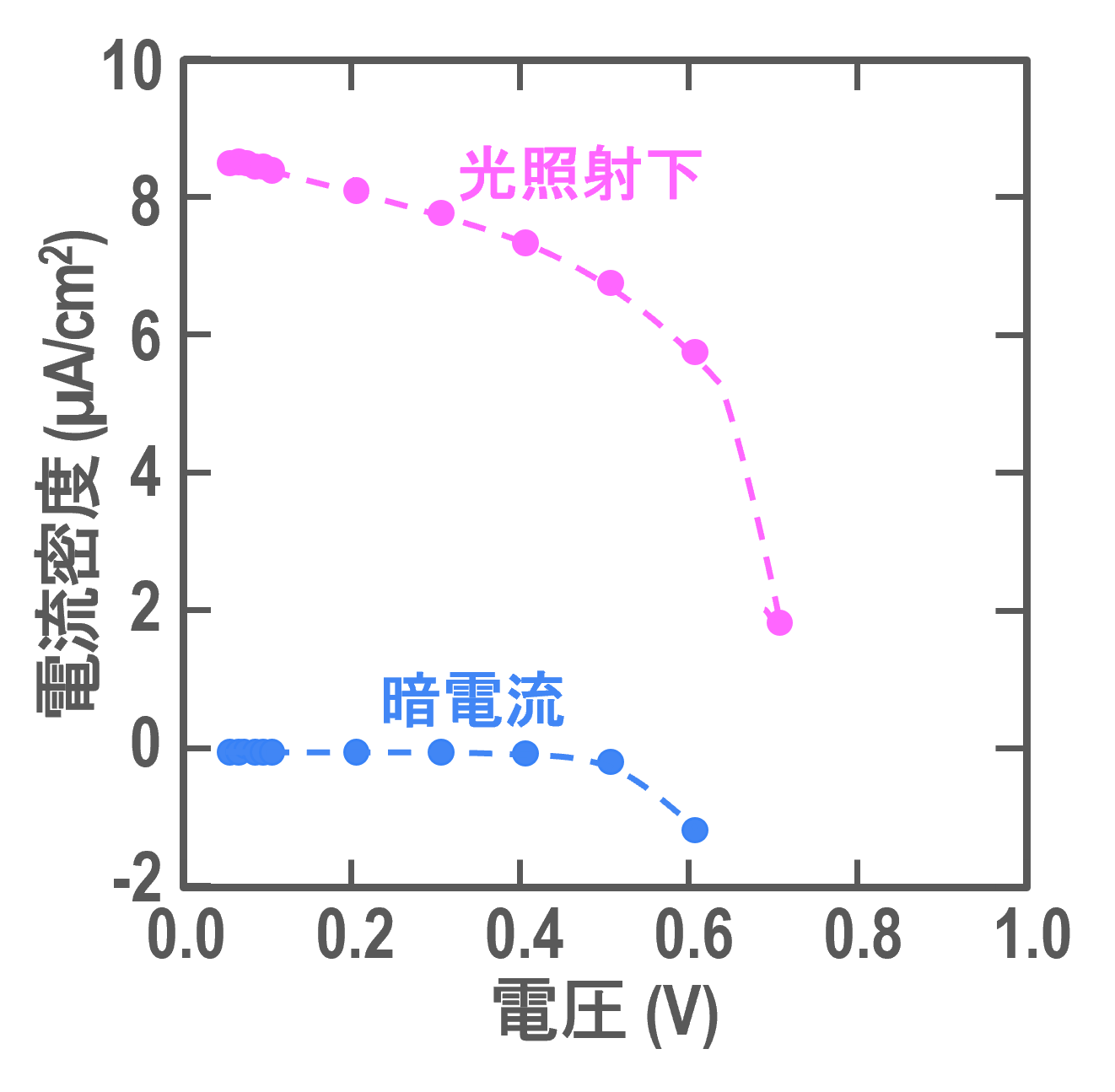
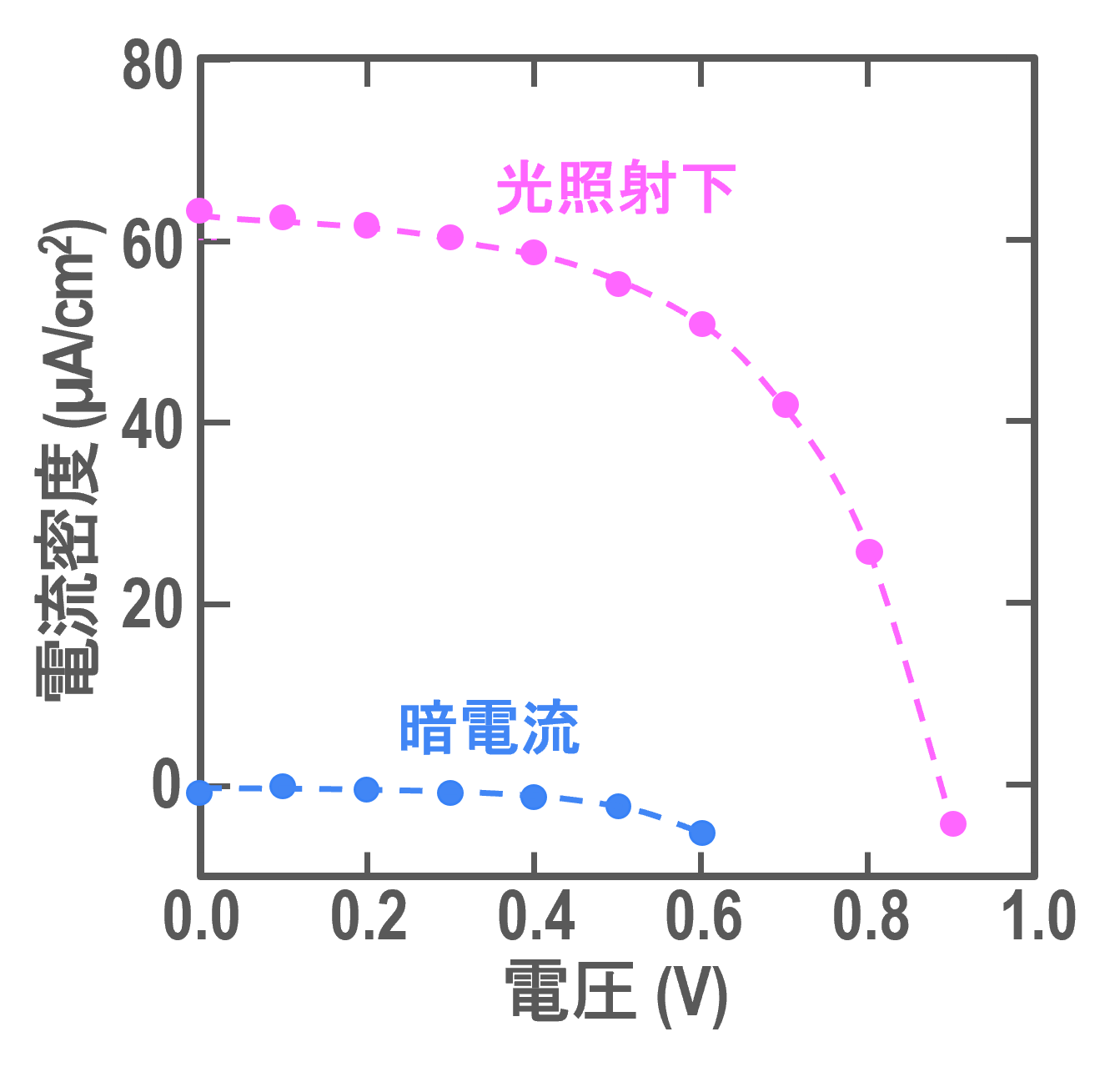
The success of N-polar GaN means the possibility of high quality InN, which is the most difficult material in nitride semiconductor because of extremely high equilibrium vapor pressure of nitrogen. In the growth of N-polarity, a nitrogen atom is caught with three gallium atoms. For III group-polarity, the situation is opposite. Therefore, by N-polar growth, the characteristics of InN can be expected to be im-proved. In near future, the properties of InN, which is not clear at present, will be precisely measured. Moreover, the device design becomes flexible because we can control the direction of spontaneous polarization.
T.Matsuoka, T. Mitate, H. Takahata, S. Mizuno, Y. Uchiyama, A. Sasaki, M. Yoshimoto, T. Ohnishi, and M. Sumiya, "N-Polarity GaN on Sapphire Substrate Grown by MOVPE", Phys. Stat. Sol. (b), 243, 1446 (2006).


.png)